This is a report from the 2022 Young Investigator Grant recipients.

Associate Professor of Electrical Engineering at Korea Advanced Institute of Science and Technology
We are living in the era of computers and smartphones. I cannot imagine work and life without having them. How have these technologies become a significant part of our life? Recall that the early stages of computers in the 1950s are made of approximately 2,000 vacuum tubes occupying the entire building space. But how about nowadays? Our tiny smartphone in your pocket has billions of transistors in one CPU! This drastic increase in the number of computing elements was the key to the advanced computing systems we utilize daily. Then, how this drastic scaling up in computing units has been realized?
The key is the integration of components like transistors and diodes in semiconductor chips. By miniaturizing each element tiny, we can put (a.k.a., integrate!) more and more computing elements in a single chip, making the computers operate at a larger scale and lower energy, lightweight, and lower unit cost. This is why all the semiconductor companies and nations, including the United States, China, and South Korea, compete to make them tiny with advanced semiconductor manufacturing technology. You probably heard the news about 5 nm and 2 nm manufacturing; it’s all about this integration issue.
Similar to electronic devices, the same analogy applies to photonic chips. Photonic integrated circuits (PICs), realized by the semiconductor manufacturing technology, utilize photons instead of electrons and miniaturize complicated, lab-scale optical systems, tiny and portable, utilizing PICs for diverse field applications. However, unlike electrons, photons behave like waves, causing significant crosstalk (i.e., exchanging optical signals and powers) between nearby devices. For example, if we place two identical strip waveguides close by, as in Fig.1(a, left), then the optical signal transfers to the other waveguide causing the noise in the signal. This coupling characteristic requires a minimum separation distance, limiting the chip integration density.
Since the rise of integrated photonics, this crosstalk and chip integration density limit has been a long-standing issue in photonics. The early stage of plasmonics in the 2000s was highlighted with the potential to resolve this issue [1,2]; still, the huge optical loss is the limit. Other dielectric approaches like optical superlattice [3] and inverse design [4] have also been proposed but with more complexity, increased scattering losses, and other practical limitations.
Around the early 2010s, in the metamaterial and metasurface community, an all-dielectric metamaterial approach emerged that utilizes low-loss dielectrics only instead of lossy metals [5]. This approach’s main advantage is the significantly reduced loss, which is promising for practical applications. Inspired by this innovative approach, I also developed a metamaterial integrated waveguide scheme, i.e., an extreme skin-depth (eskid) waveguide [Figs.1(a, right) and 1(c)] [6,7]. The subwavelength gratings (SWGs) in the cladding form highly anisotropic metamaterials and reduce the skin depth of the evanescent waves. The right panel of Fig.1(a, right) illustrates the conceptual image of the eskid waveguide, and Fig. 1(c) shows the fabricated scanning microscopic (SEM) image. By engineering the geometric parameters of SWGs, the anisotropic optical properties in the cladding can be changed, reducing the crosstalk when two or more waveguides are proximate and coupled. Using the highly anisotropic SWGs, two fundamental optical phenomena, i.e., skin-depth engineering [6] and anisotropic perturbation for exceptional coupling [7], were found, demonstrating the record-long coupling length. This approach, however, worked with only transverse electric (TE) polarization.
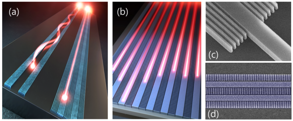
In general, PICs utilize both TE and transverse-magnetic (TM) polarizations. Due to PIC’s asymmetric width-to-height aspect ratio, each mode exhibits different modal properties and usage. For example, TM is widely used for optical sensing with its vertically extended skin depth. The TM mode’s less confinement makes it easier to interact with nearby devices, which is, at the same time, not ideal for dense integration. The research goal of the Yong Investigator Grant (YIG), supported by the Korean-American Scientists and Engineers Association (KSEA), was to overcome this TM crosstalk challenge. Here the orientation of SWGs is rotated, forming orthogonal anisotropic metamaterials compared to the eskid waveguide. Figure 1(b) illustrates the conceptual SWG waveguides for TM crosstalk suppression, and Fig. 1(d) shows the fabricated SEM image. With this scheme, the TM mode forms leaky-like oscillations in the SWG claddings, achieving zero crosstalk via anisotropic perturbation [8]. It is counter-intuitive to achieve a zero crosstalk with a leaky mode since a leaky mode typically shows a strong coupling even at far distances with its radiative waves. However, by engineering the anisotropic optical properties of SWGs, dielectric perturbations could cancel out couplings from each field component and achieve zero crosstalk completely. This non-trivial coupling phenomenon was experimentally demonstrated, suppressing the crosstalk talk by more than two orders of magnitude [8]. Since we have shown this on a conventional silicon-on-insulator (SOI) platform, the scheme is directly applicable to other applications with much higher chip integration density for TM polarization.
Note that the SWG schemes introduced here are just simple basic waveguide schemes. By utilizing these schemes as unit modes, various optical components can be developed with a smaller size. For example, PIC components like high extinction-ratio polarization beam splitter (PBS) [9] and broadband PBS [10] are developed, and other components like densely packed integrated delay lines and polarization splitters and rotators are under development. More exciting research opportunities can also be explored with other SWG metamaterials, like tilted and bianisotropic schemes, toward achieving high-density photonic chip integration.
References
[1] E. Ozbay, “Plasmonics: merging photonics and electronics at nanoscale dimensions” Science 311, 189-193 (2006)
[2] R. Oulton, V. Sorger, D. Genov, D. Pile, and X. Zhang, “A hybrid plasmonic waveguide for subwavelength confinement and long-range propagation” Nature Photonics, 2, 496-500 (2008)
[3] W. Song, R. Gatdula, S. Abbaslou, et al. “High-density waveguide superlattices with low crosstalk” Nature Communications 6, 7027 (2015)
[4] M. Mrejen, H. Suchowski, T. Hatakeyama, et al. “Adiabatic elimination-based coupling control in densely packed subwavelength waveguides” Nature Communications 6, 7565 (2015)
[5] S. Jahani and Z. Jacob, “All-dielectric metamaterials” Nature Nanotechnology 11, 23-36 (2016)
[6] S. Jahani, S. Kim, J. Atkinson, et al. “Controlling evanescent waves using silicon photonic all-dielectric metamaterials for dense integration” Nature Communications 9, 1893 (2018)
[7] M. Mia, S. Ahmed, I. Ahmed, Y. Lee, M. Qi, and S. Kim, “Exceptional coupling in photonic anisotropic metamaterials for extremely low waveguide crosstalk” Optica 7, 881-887 (2020)
[8] M. Kabir, M. Mia, I. Ahmed, N. Jaidye, S. Ahmed, and S. Kim, “Anisotropic subwavelength grating perturbation enables zero crosstalk in a leaky mode” arXiv:2210.08741 (2022)
[9] S. Ahmed, I. Ahmed, M. Mia, N. Jaidye, and S. Kim, “Ultra-high extinction ratio polarization beam splitter with extreme skin-depth waveguide” Optics Letters 46, 2164-2167 (2021)
[10] M. Mia, S. Ahmed, N. Jaidye, I. Ahmed, and S. Kim, “Mode-evolution-based ultra-broadband polarization beam splitter using adiabatically tapered extreme skin-depth waveguide” Optics Letters 46, 4490-4493 (2021)
